BASIC PHOTOPHYSICS
Antonie J.W.G. Visser1,2 (1943-2018) and Olaf J. Rolinski2
1Laboratory of Biochemistry, Microspectroscopy Centre
Wageningen University, P.O. Box 8128
6700 ET Wageningen, The Netherlands
antoniejvisser@gmail.com
2Department of Physics, University of Strathclyde
Scottish Universities Physics Alliance, Photophysics Group
Glasgow G4 0NG, UK
o.j.rolinski@strath.ac.uk
Introduction
Basic photophysics in the framework of photobiology is concerned with processes that occur when sunlight, filtered through the Earth's atmosphere, interacts with matter (atoms and molecules) present on Earth. The spectrum of solar radiation striking the Earth (Figure 1) spans 100 nm to 106 nanometers (1 nm = 10-9 m) and can be divided into the ultraviolet (UV) range (100 nm to 400 nm), visible range (400 nm to 700 nm) and infrared (IR) range (700 nm to 106 nm). UV radiation has both damaging and beneficial effects on living matter. UV radiation is also responsible for the photochemical reaction leading to production of the protective ozone layer in the atmosphere. As the name suggests the visible part of the spectrum is the light that human eyes can detect. An important part of electromagnetic radiation reaching the Earth is IR radiation.
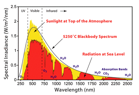
Figure 1. Solar radiation spectrum above the atmosphere, and at the surface of the earth. [From Wikipedia: Sunlight]
The spectrum of solar radiation is close to that of a black body with a temperature of 5600 K. A black body is an idealised object that absorbs all electromagnetic radiation falling on it. Because no light is reflected or transmitted, the object appears black when it is cold. However, a black body emits a temperature-dependent spectrum of light, which is termed black-body radiation. All hot objects radiate a mixture of heat and light, with intensity and color varying with temperature. Think of an iron poker in a fire that changes color when it becomes hotter, and after taking it out the glow starts to disappear, as does the heat. Historically, studying the laws of black-body radiation has led to the development of quantum mechanics.
Visible light is only one small part of the electromagnetic spectrum, which is classified by wavelength into radio wave, microwave, infrared, visible, ultraviolet, X-rays and gamma rays (Figure 2).
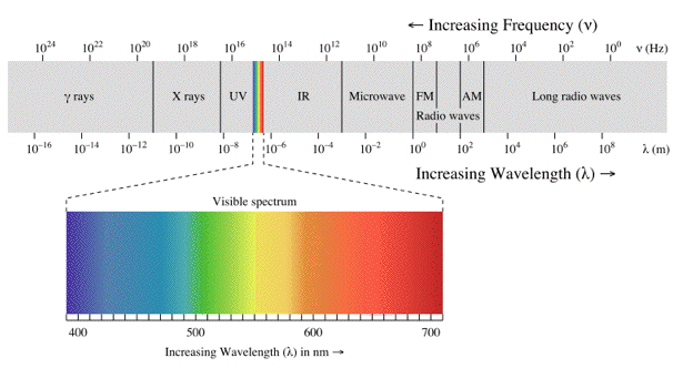
Figure 2. Electromagnetic spectrum, with the visible light spectrum enlarged. [From Wikipedia: Electromagnetic Radiation]
The behaviour of electromagnetic radiation depends on its wavelength or energy (i.e., frequency). Higher frequencies have shorter wavelengths and, vice versa, lower frequencies have longer wavelengths. The interaction of electromagnetic radiation with atoms or molecules depends on the energy. Spectroscopy can be detected at a much wider range than the visible range of 400 nm to 700 nm. Depending on the spectral region of interest, the units used to describe the radiation may be frequency, energy, wavelength or inverse wavelength (wavenumber). Table 1 compares different spectral regions.
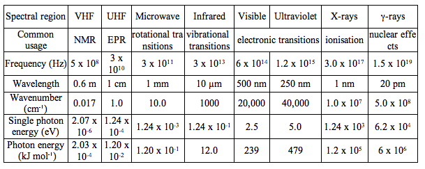
Table 1. Characteristics of the Electromagnetic Spectrum. Wavelength ranges of the electromagnetic spectrum have been classified by their spectroscopic uses. For example, very high frequency (VHF) radiation is used in nuclear magnetic resonance (NMR), while ultra high frequency (UHF) radiation is used in electron paramagnetic resonance (EPR). The other rows of Table 1 provide information on frequency, wavelength, wave number and energy for a center wavelength of the spectral range. The last row gives the energy provided by one mole of photons of given wavelength, that is the energy per einstein.
Electromagnetic radiation exhibits both wave-like and particle-like properties, a concept known as wave-particle duality. Both wave and particle characteristics have been demonstrated by a large number of experiments. Electromagnetic waves are composed of an electric field (E), and a magnetic field (B) perpendicular to it, oscillating in phase in the propagation direction (k). An arrow on top of a letter gives the direction of the vector (Figure 3).

Figure 3. Electromagnetic waves as oscillating electric and magnetic fields. (-q and +q represent electrical charges)
[From Wikipedia: Electromagnetic Radiation]
The sinusoidal waves are characterized by frequency ν, which is inversely proportional to the wavelength λ according to the equation:

where c is the speed of light (in vacuum c = 300,000 km/s; light travels in one nanosecond 30 cm; 1 ns =10-9 s). The wave model can explain several phenomena. Interference is the superposition of two waves giving a new wave pattern that can be constructive when two waves have the same direction or destructive when they have the opposite direction. Another example is light dispersion into a visible spectrum when white light is shone through a prism, because of the wavelength dependent refractive index of the prism material. Electromagnetic waves also have particle-like properties, as packets of energy or quanta, called photons. The energy per photon, E, can be calculated from the Planck-Einstein equation:

where h is Planck's constant and ν is frequency. The particle model can explain the absorption and emission spectra of light by atoms or molecules. The absorption of electromagnetic radiation is how photon energy is taken up. Typically an electron is elevated to a higher energy level by light absorption. When an excited electron returns to the lowest energy level, a light photon is emitted.
Molecular Photophysical Processes Relevant for Photobiology
Molecular photophysical processes relevant for photobiology include absorption and emission of UV, visible or near-IR light, by aromatic molecules. In the remainder of this module we will focus on these processes.
Jablonski Diagram: Basic principles of molecular photophysics can be clarified with the help of the Jablonski diagram, named after the Polish physicist Aleksander Jablonski (Figure 4).

Figure 4. Jablonski diagram representing energy levels and spectra. Solid arrows indicate radiative transitions as occurring by absorption (violet, blue) or emission (green for fluorescence; red for phosphorescence) of a photon. Dashed arrows represent non-radiative transitions (violet, blue, green, red). Internal conversion is a non-radiative transition, which occurs when a vibrational state of a higher electronic state is coupled to a vibrational state of a lower electronic state. In the notation of, for example, S1,0, the first subscript refers to the electronic state (first excited) and the second one to the vibrational sublevel (v = 0). In the diagram the following internal conversions are indicated: S2,4→S1,0, S2,2→S1,0, S2,0→S1,0 and S1,0→S0,0. The dotted arrow from S1,0→T1,0 is a non-radiative transition called intersystem crossing, because it is a transition between states of different spin multiplicity. Below the diagram sketches of absorption-, fluorescence- and phosphorescence spectra are shown.
The diagram illustrates the electronic states of a molecule and the transitions between them. The electronic states are arranged vertically by energy. They are grouped horizontally by spin multiplicity. In the left part of the diagram three singlet states with anti-parallel spins are shown: the singlet ground state (S0) and two higher singlet excited states (S1 and S2). Singlet states are diamagnetic, as they do not interact with an external magnetic field. The triplet state (T1) is the electronic state with parallel spins. A molecule in the triplet state interacts with an external magnetic field. Transitions between electronic states of the same spin multiplicity are allowed. Transitions between states with different spin multiplicity are formally forbidden, but may occur owing to a process called spin-orbit coupling. This transition is called intersystem crossing. Superimposed on these electronic states are the vibrational states, which are of much smaller energy. In the following sections we will address the sequence of processes, which occur when an aromatic molecule absorbs a photon of sufficient energy.
It requires some effort to calculate the energy levels and wavefunctions of an aromatic molecule of average size. Born and Oppenheimer have made this task considerably easier by breaking up the quantum-mechanical wavefunction of a molecule into its electronic and nuclear (vibrational and rotational) components:

In the first step of this Born-Oppenheimer approximation the electronic Schrödinger equation is solved yielding the electronic wavefunction,
 , depending on electrons only with the nuclei fixed in an equilibrium configuration.
Light Absorption: When a molecule absorbs a photon of appropriate energy, a valence electron is promoted from the ground state to some vibrational level in the excited singlet manifold (Figure 4). The process of light absorption is extremely rapid, in the order of one femtosecond (1 fs = 10-15 s). It means that the nuclei of the molecule are fixed during the transition, because of their much larger mass, and that the Born-Oppenheimer approximation is valid.
It is to be noted that the point of departure is always the lowest vibrational level of S0 designated S0,0. We can understand this by referring to the Boltzmann distribution function, which is a measure for the distribution of (in this case) vibrational states of the molecule:

where N1 is the number of molecules in the first higher vibrational state (S0,1), and N0 that for the lowest vibrational level (S0,0), ΔEvib is the energy difference between the two vibrational states, kB is the Boltzmann constant, and T the absolute temperature. At room temperature, ΔEvib is much larger than kBT, implying that only the lowest vibrational level is populated.
After light absorption the excited molecule ends up at the lowest vibrational level of S1 (S1,0) via vibrational relaxation and internal conversion. This radiationless process takes place in about one picosecond (1 ps = 10-12 s).
A sketch of an absorption spectrum consisting of two bands is shown in Figure 4. In the condensed phase, broad absorption (and also emission) bands are observed, not the sharp transitions seen for atoms or molecules in the gaseous phase. The reason is due to phenomena known as homogeneous broadening and inhomogeneous broadening. Homogeneous broadening arises from the multitude of vibrational states (many more than shown in Figure 4) and rotational states (superimposed on the vibrational states), which all are superimposed on the electronic transitions preventing the observation of sharp transitions. Inhomogeneous broadening arises from solvent effects, which will be detailed later for fluorescence.
The strength of the lowest optical transition is very often expressed in terms of the (dimensionless) oscillator strength f:

where ε is the molar extinction coefficient connected with the lowest electronic transition, σ is the wavenumber and the integral is over all wavenumbers of the absorption band. For intense (strongly allowed) transitions f ≈ 1. The oscillator strength has a direct relationship with the electronic transition dipole μeg, which couples the wavefunctions of the ground (ψg) and excited (ψe) electronic states:

with μ=-er (e is charge of electron), and the integration takes place over spatial coordinates r.
The transition dipole is a measure of the dipole moment associated with the shift of charge that occurs when electrons are redistributed in the molecule upon excitation. The oscillator strength is proportional to the magnitude of the transition dipole:

Fluorescence: In 1852, the British scientist Sir George G. Stokes coined the term "fluorescence" after observing blue luminescence in the mineral fluorite. Stokes also discovered the redshift in band maximum of the fluorescence spectrum relative to the band maximum of absorption (Stokes shift).
The lowest vibrational level of S1 is the starting point for fluorescence emission to the ground state S0, non-radiative decay to S0 (internal conversion), and transition to the lowest triplet state (intersystem crossing) (Figure 4). Fluorescence takes place on the nanosecond timescale (1 ns = 10-9 s) and, depending on the molecular species, its duration amounts to 1-100 nanoseconds. It is clear from the Jablonski diagram that fluorescence always originates from the same level, irrespective of which electronic energy level is excited. The emitting state is the zeroth vibrational level of the first excited state S1,0. It is for this reason that the fluorescence spectrum is shifted to lower energy than the corresponding absorption spectrum (Stokes shift). The Stokes shift can be enhanced by solvent interactions, examples of which will be given later. We can also conclude from the sketched spectra in Figure 4 that vibrational fine structure in a fluorescence spectrum reports about vibrations in the ground state, and vibronic bands in an absorption spectrum provides information on vibrations in higher electronic excited states.
Another factor that has to be considered in fluorescence spectroscopy is the Franck-Condon factor. If we look at the Jablonski scheme in Figure 4, it can be seen that the fluorescence transition S1,0→S0,0 is not the most intense one. The Franck-Condon principle states that the most intense vibronic transition is from the vibrational state in the ground state to that vibrational state in the excited state vertically above it (Figure 5, blue arrow).

Figure 5. Energy diagram for explanation of the Franck-Condon principle. The potential wells show favored transitions between vibrational sublevels ν = 0 and v = 2 both for absorption (blue arrow) and emission (green arrow).
[From Wikipedia: Franck-Condon Principle]
The schemes (for absorption and emission) in Figure 5 are simplified two-dimensional potential energy diagrams, but for the sake of argument, they are a sufficient representation, since we are dealing with (an)harmonic oscillators. Since the excited state is different from the ground state, a displaced minimum nuclear normal coordinate can be expected. It should be noted further that the time to reach the excited state is so short (femtoseconds) that the nuclei positions are virtually unchanged during the electronic transition. In the vibronic wavefunctions, the nuclear coordinates can then be uncoupled from the electronic coordinates (Born-Oppenheimer principle). The transition dipole can then be factored into an electronic and a nuclear part:

The second integral is the so-called Franck-Condon vibrational overlap, which also determines the strength of the electronic transition (or oscillator strength). In the fluorescent part of the scheme in Figure 4, the second and third vibrational transitions (S1,0→S0,1 and S1,0→S0,2) have larger Franck-Condon factors than the one between fundamental vibrational wavefunctions (S1,0→S0,0).
Phosphorescence: In Figure 4, the triplet state is also drawn. Once the molecule has reached this state, it will reside for a very long time there (from microseconds to seconds) before it will decay to the ground state. This is due to the spin-forbidden transitions involved in the (excited) singlet-triplet and triplet-singlet (ground state) transitions. In rigid solution or in deoxygenated solutions, long-lived phosphorescence (milliseconds to seconds) from this state can be observed. The name "phosphorescence" probably originates from the French physicist Edmond Becquerel, who devised in 1857 an instrument that he called a phosphoroscope. With this instrument he could measure how long it takes a phosphorescent sample to stop glowing after excitation.
Because of its long lifetime, the triplet state of an aromatic molecule is the starting point for photochemical reactions. One reaction in particular is very prominent, namely the production of very reactive singlet oxygen. The oxygen molecule, O2, possesses a triplet ground state. In solution, frequent collisions between an aromatic molecule in the triplet state and oxygen result in energy transfer, and generation of singlet oxygen, which can oxidise (and destroy) the aromatic molecule.
Practical Aspects of Fluorescence
[see Module on Basic Spectroscopy]
Absorption Spectrum: The measurement of an absorption spectrum (Figure 6) is based on the Lambert-Beer law, and shows the ability of the investigated sample to absorb light at different wavelengths. As light absorption occurs almost always from the lowest vibrational level of the electronic ground state, the absorption spectrum characterizes the energetic structures of the electronic excited states of an aromatic molecule.
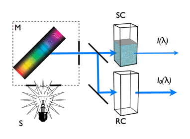
Figure 6. Measurement principle of light absorption spectra. The values measured directly in the spectrophotometer are the intensities of light transmitted through sample and reference cuvettes.The light source S generates a broad spectrum of light and the dispersion device (grating or prism) M selects a monochromatic light of specific wavelength λ. The light is then divided into two identical beams directed to two cuvettes, a sample cuvette, SC, containing the solution of the aromatic compound and a reference cuvette, RC, with solvent only. Changing the wavelength over the required range enables measuring the intensities of the light transmitted through both cuvettes, I(λ) and I0(λ).
The absorbance Aλ at wavelength λ is then defined as:

and is equal according to the Lambert-Beer law to:

where ε(λ) is the extinction coefficient at wavelength λ for the particular molecule, c its concentration, and d the path length of the cuvette, for instance 1 cm.
Examples of absorption (absorbance, left side) and fluorescence (right side) spectra of three widely investigated fluorophores are presented in Figure 7.

Figure 7. Normalised absorption (left), and fluorescence (right) spectra of three fluorophores. Shown are the spectra of 2,5-diphenyl-oxazole (PPO, a molecule used in scintillation counting) in an organic solvent, N-acetyl-tryptophan amide (NATA), and the protein human serum albumin (HSA) in aqueous buffer.
Fluorescence Spectrum: A fluorescence spectrum Iflu(λ) represents the intensity of the fluorescence light emitted by the sample as a function of emission wavelength (Figure 8). As fluorescence transitions start in most cases from the lowest vibrational level of the first electronic excited state, Iflu(λ) characterises the energetic structure of the electronic ground state.
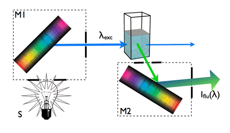
Figure 8. Measurement of fluorescence spectra.
Fluorescence is detected at right angle to the excitation beam. A monochromatic light beam of selected wavelength λexc excites the molecules in the sample. Fluorescence light is emitted from the excited state of these molecules in all directions. Fluorescence is usually collected at right angles to the excitation direction in order to minimize the presence of scattered excitation light in the fluorescence channel. The monochromator M2 allows measurements of fluorescence intensity as a function of the emission wavelength. The fluorescence spectra of PPO, NATA and HSA are shown in Figure 7.
Sometimes it is useful to measure how fluorescence intensity depends on the excitation wavelength. In this case we will detect fluorescence intensity at a fixed wavelength (for instance at the wavelength of maximal fluorescence) as a function of the excitation wavelength (M1), thus obtaining an excitation spectrum. An excitation spectrum is essentially an absorption spectrum, because the fluorescence intensity Iflu(λ) is proportional to:

where ε(λ) is the extinction coefficient at excitation wavelength λ, I0 is the monochromatic light intensity, and Φ is the quantum yield of fluorescence (see below). This equation is valid only for dilute fluorophore solutions, in which the absorbance of the aromatic compound never exceeds 0.05. Excitation spectra turn out to be useful in obtaining absorption spectra of very dilute samples.
Quantum Yield of Fluorescence: The quantum yield, Φ, is defined as the ratio of the number of fluorescence photons emitted by the sample nE to the number of photons absorbed nA. It can be shown also that Φ is the ratio of the rate of the radiative transition (kr) to the rates of all transitions (kr+knr), in which the excited state is involved. Therefore, any molecular mechanism leading to a non-radiative depopulation of the excited state reduces the quantum yield:

The quantum yields of some popular fluorophores, naturally occurring mono- and dinucleotides, wild type green-fluorescent protein (GFP), and other visible fluorescent protein variants, are collected in Table 2.
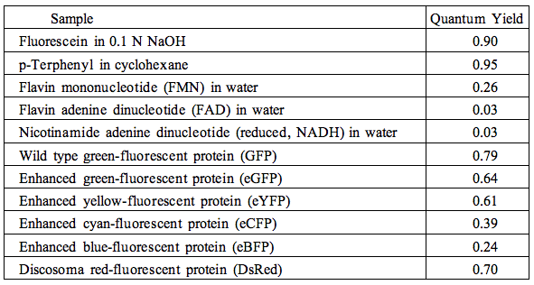 Table 2. Quantum yields of selected fluorophores.
Fluorescence Lifetime: The other important characteristic feature of fluorescence is its time response, namely the decay of fluorescence intensity following infinitesimally short or δ-type excitation. The scheme presented in Figure 9 is a simplified Jablonski diagram, which can be used to explain the basic kinetics of fluorescence.

Figure 9. Kinetic scheme to explain fluorescence lifetime. δ(0) is excitation with a δ-pulse, kr is rate constant of radiative transition, and knr is rate constant of non-radiative transition.
The population of the excited molecules [M*] generated at the moment of excitation, t=0, starts to decrease exponentially through the radiative (kr) and non-radiative (knr) transitions to the ground state.
The characteristic time of this process,
 0, is called the fluorescence lifetime:

The intensity of fluorescence, F(t), emitted at any moment of this process is proportional to [M*](t), thus:

Note that F(t) is a shorthand notation for Iflu(t). The fluorescence lifetime
 0 has the physical meaning of the time needed for the fluorescence intensity to decrease to 1/e (= 1/2.71) of its initial value F0 (Figure 10).
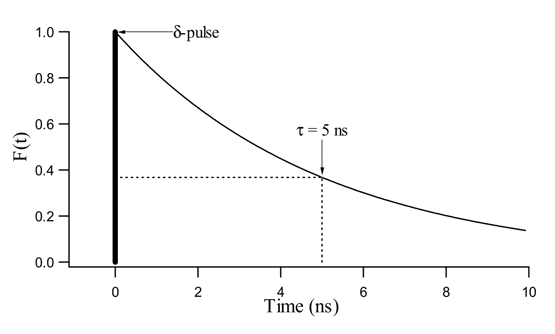
Figure 10. Fluorescence decay F(t) = F0 exp(-t/5) with t in ns. F(t) is the fluorescence intensity that decays exponentially with a fluorescence lifetime,0, equal to 5 ns. The δ-pulse represents an excitation light pulse of infinitesimally small duration, for instance, a duration of 1 femtosecond (10-15 second).
In practice the generation of a δ-pulse for excitation is not possible, because the instrumental response time needed to detect fluorescence decays is often comparable to the fluorescence lifetimes that we want to measure. The experimentally detected fluorescence decays are not pure decays like F(t) in Figure 10, but convolutions of the ideal decay function with the so called prompt function (or instrumental response function). Measuring the prompt function, and then extracting the undistorted fluorescence decay function will be described later in this module.
Fluorescence Anisotropy: Photons can be absorbed only when their energy fits to the energy gap between the ground and excited energy levels of a particular molecule. Another condition for light absorption is that the electric component or vector of the electromagnetic wave must be parallel or close to parallel, to the transition moment of the molecule.
In solution, the orientations of the transition moments are completely random. Therefore, if we excite such a system with linearly polarized light, the excitation will be efficient only for those molecules whose transition moments are, at the moment of excitation, oriented similarly to the direction of polarization. The initial distribution of orientations of the excited molecules will then be highly anisotropic. This ordering effect is called 'photoselection'.
After excitation, the molecules start to fluoresce with their characteristic fluorescence lifetime
 0, and, simultaneously, Brownian rotational motion causes the initial orientational order of the excited molecules to vanish.
Polarization of fluorescence is determined by the orientation of the fluorophores' transition moment at the instant of fluorescence emission. This gives an opportunity to determine rotational diffusion of fluorophores by detecting the anisotropy of their fluorescence (Figure 11).
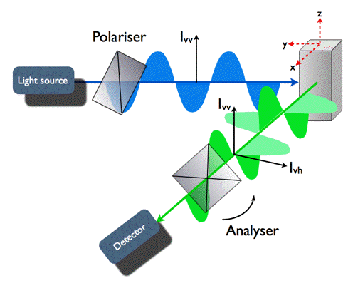
Figure 11. Geometry of fluorescence anisotropy experiment. Fluorophores in the cuvette are excited with short pulses of vertically polarized light (z) causing photoselection. A polarizer in the fluorescence channel (x) can be rotated from the vertical to the horizontal position. In the first part of the experiment, the decay of intensity of vertically polarized fluorescence Ivv(t) is measured. Then the polarizer is moved to horizontal orientation, and Ivh(t) is detected.
Both decays, Ivv(t) and Ivh(t), are combined to form the fluorescence anisotropy function r(t), defined as:

For spherical and freely rotating fluorophores the anisotropy decays exponentially:

with the characteristic decay constant
 r, called rotational correlation time, and r0 = 2/5 for randomly distributed molecular systems. According to the theory of rotational diffusion,
  r is related to the radius r of a rotating sphere by the equation:

Here, kBT is the Boltzmann factor, and η is the viscosity of the solvent. The relation between fluorescence anisotropy decays, and the dimensions of rotating molecules is one of the fundamentals of the newly emerging research discipline of 'nanometrology'.
Solvent Effects on Fluorescence: The concept of solvation can be understood from interactions between a fluorophore (the solute), and the surrounding solvent molecules. The dominating solute-solvent interactions arise from electrostatic dipole-dipole interactions, which lead to lowering the potential energies of all energy levels involved in absorption and fluorescence processes. This effect can be explained by Onsager's model of solvation (Figure 12).
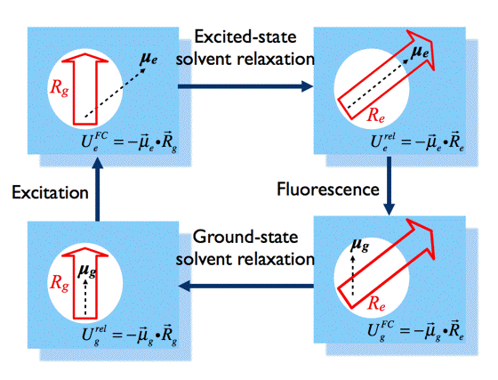
Figure 12. Changes in solute-solvent interactions lead to solvatochromic shifts in absorption and fluorescence spectra of the same fluorophore. [see text for definitions of symbols]
According to this model, the dipole moment of the fluorophore in the ground state, μg, interacts with the dipole moments of the surrounding solvent molecules, rearranging them in a way that minimises the potential energy of the whole system. If we would "freeze" the molecules for a while and remove the fluorophore, the special arrangement of the solvent dipole moments would result in a non-balanced electric field Rg, called the "reaction field".
In Onsager's model, the solute-solvent interaction is identified as an interaction of the fluorophore dipole moment, μg, with the reaction field Rg, namely:

The energy level of the ground state is therefore lowered by this value. The symbol 'rel' indicates that the solvent is in a state of thermodynamic equilibrium (relaxed). Electronic excitation of the fluorophore (Figure 12) causes a rapid (~10-15 s) change of its dipole moment to μe. This time is much too short for the solvent molecules to rearrange their orientations. Thus, immediately after excitation the interaction energy will be:

indicating that the reaction field will be still the same as it was before excitation. The symbol 'FC' indicates a non-equilibrated, Franck-Condon state. The solvent molecules need usually picoseconds (10-12-10-10 s) to perform solvent relaxation achieving finally the solute-solvent interaction energy:

The process of fluorescence brings the fluorophore dipole moment back to its ground-state value μg, so just after fluorescence:

which finally evolves during ground-state solvent relaxation to
 .
.
Direct consequences of the different solute-solvent interaction energies at different stages of absorption and fluorescence events are the spectral shifts in absorption (ΔUabs) and fluorescence (ΔUflu) spectra:

The fluorescence spectra of the solvent-sensitive fluorophore "badan" in a number of solvents are shown in Figure 13. For "badan", μe is much larger than μg. The larger the dipole moment of the solvent molecule the stronger is the "red-shift" of the spectrum.

Figure 13. Fluorescence spectra of "badan" (i.e., the 2-mercapto-ethanol adduct of 6-bromoacetyl-2-dimethylaminonaphtalene) in: (1) toluene, (2) chloroform, (3) acetonitrile, (4) ethanol, (5) methanol and (6) water. Figure from Handbook of Molecular Probes.
Quenching of Fluorescence by External Molecules: Any molecule that interacts with the fluorophore and reduces its quantum yield, is called a quencher. There are a number of different molecular mechanisms of quenching.
In case of static quenching, external molecules Q, simply form ground-state complexes with the fluorophore M (Figure 14). These complexes can be excited, but are not fluorescent.
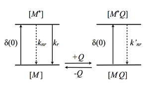
Figure 14. Schematic illustration of static quenching. The MQ complex is not fluorescent yielding reduction in fluorescence intensity, but no change in fluorescence lifetime (see text).
The equilibrium between free and complexed fluorophores is controlled by an association constant Ks:

where [M], [Q] and [MQ] are the concentrations of fluorophore, quencher and fluorophore-quencher complexes, respectively. [M]0 is the total concentration of the fluorophore. The above equation can be easily converted into the well-known Stern-Volmer equation, which describes the decrease of fluorescence intensity with increasing quencher concentration:

Here, F0 and F are the fluorescence intensities measured without, and in the presence of the quencher. Due to the nature of static quenching, there is no change in fluorescence lifetime, since only the non-complexed fluorophore is fluorescent. However, the quencher-fluorophore complex can still be fluorescent, but displays an ultra-short fluorescence lifetime in the picosecond time-range yielding no significant steady-state fluorescence intensity. The static quenching arises from competing processes that induce non-radiative pathways to the ground state. The non-radiative rate constant (k'nr) is much larger than the radiative rate constant (kr), and emission is almost completely eliminated.
In the case of dynamic quenching the quenching molecule Q collides with the excited fluorophore M* (Figure 15). The excited state kinetics are affected by forming an additional way of depopulating the excited state. Consequently, the fluorescence decay is modified. Both steady-state and time-resolved fluorescence yield the famous Stern-Volmer constant
KSV =
 0kq, in which
  o is the fluorescence lifetime without quencher, and kq is the diffusion controlled rate constant of quenching. KSV has the dimension M-1.
Several compounds behave as dynamic quenching agents when present at sufficiently high concentration, including oxygen, heavy-atom halides such as bromide and iodide, mercury and caesium ions, tetrachloro-methane (CCl4), amines and acrylamide.
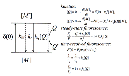
Figure 15. Schematic illustration of dynamic quenching and relevant rate equations. The steady-state fluorescence intensity ratio (F0/F) (F is the fluorescence intensity in presence of quencher Q) is the same as the ratio of fluorescence
lifetimes0/
q (
q is the fluorescence lifetime in the presence of quencher Q). The Stern-Volmer constant KSV is equal to
0kq.
Förster Resonance Energy Transfer (FRET): Theodor Förster developed the quantitative theory for resonance energy transfer in the late 1940s. Therefore, we call this process Förster resonance energy transfer or FRET. FRET is a photophysical process where the excited-state energy from a donor molecule is transferred non-radiatively to an acceptor molecule at close distance via weak dipole-dipole coupling (Figure 16). FRET is sometimes referred to as "fluorescence" resonance energy transfer, but this is a misconception, since no fluorescence takes part in the coupled transition.
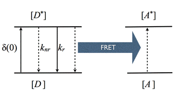
Figure 16. Kinetic scheme of FRET.
Förster derived the following expression for the rate constant of transfer kT:

in which R is the distance between donor and acceptor molecules and
 D is the fluorescence lifetime of the donor (without acceptor). Since the transfer rate is proportional to the inverse 6th power of the distance R, the transfer rate is an extremely sensitive parameter for obtaining distances in the range of 1-10 nm (or 10-100 Å). The distance at which the excitation energy of the donor is transferred to the acceptor with probability 0.5, is called the Förster or critical distance R0 (in units of cm), and can be calculated using the relevant spectroscopic properties of the participating molecules:

in which κ2 is the orientation factor, Φ0 the quantum yield of donor fluorescence (without acceptor), NA is Avogadro's number, and n is the refractive index of the intervening medium. The integral (J, in units of M-1cm3) is the degree of spectral overlap between donor fluorescence spectrum (FD, its spectrum normalized so that the integral is equal to one), and acceptor absorption spectrum (scaled to its maximum molar extinction coefficient, εA, in units of M-1cm-1), given by either wavenumber (σ) or wavelength (λ) scale (Figure 17):

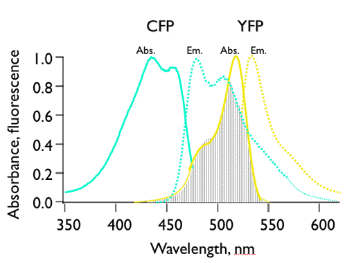
Figure 17. Illustration of spectral overlap integral between the fluorescence spectrum of cyan-fluorescent protein (CFP), and the absorption spectrum of yellow-fluorescent protein (YFP). CFP and YFP are mutants of Green Fluorescent Protein.
The orientation factor κ2 is given by:

For a definition of the angles we refer to Figure 18, in which some limiting situations have been depicted illustrating that 0 < κ2 < 4. For systems without any 3-dimensional, spatial information the orientation factor is the indeterminate parameter in R0. All other parameters can be measured or evaluated.

Figure 18. The orientation factor in FRET. μD and μA are the transition moments of donor and acceptor molecules and R is the separation vector.
When the critical transfer distance, R0 (see equation above), is expressed in units of Å, the scaling constant
 is equal to 0.2108, the molar extinction coefficient, εA, in units of M-1cm-1, the wavelength, λ, in units of nm, and the overlap integral, J, in units of
 M-1cm-1nm4, and R0 is given by:

For an exercise how to calculate the critical transfer distance from spectroscopic data see Module in Experiments for Students: (A.J.W.G. Visser, E.S. Vysotski and J. Lee)
Förster also introduced the transfer efficiency E, which is only a function of actual (R) and critical (R0) distances:

There are several methods available for quantification of FRET, of which the one based on donor fluorescence lifetimes is the most straightforward, because the fluorescence lifetime is a concentration-independent property, while fluorescence intensity is not. Donor fluorescence lifetimes in the absence (
 D) and presence (
 DA) of acceptor molecules are often measured for the observation of FRET and a decreased fluorescence lifetime of the donor is then an indication of molecular interactions (Figure 19). From this reduction in lifetimes we immediately obtain the experimental FRET efficiency:

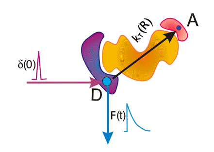
Figure 19. Time-resolved fluorescence detection of FRET. Shown are a donor molecule D and an acceptor molecule A separated at distance R in a macromolecule. A very short light pulse (δ(0)) excites donor D. Analysis of the generated donor fluorescence decay (F(t)) gives information on the rate constant of transfer κT from which the distance R can be obtained.
In Figure 20 we have summarised the main concepts of FRET, which are illustrated with the widely used FRET couple CFP (cyan-fluorescent protein, donor) and YFP (yellow-fluorescent protein, acceptor). FRET is used extensively for monitoring interactions and conformational changes between or within biological macromolecules conjugated with suitable donor-acceptor pairs. Because of its sensitivity FRET also forms the basis for "sensing" important biological molecules in many applications.
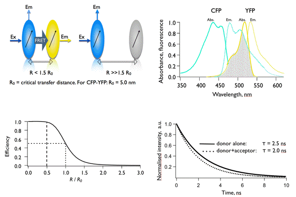
Figure 20. Main concepts of FRET. The occurrence of FRET depends on distance (upper left panel) and the spectral overlap (upper right panel). The reduction of a lifetime from 2.5 to 2.0 ns corresponds to a transfer efficiency of 0.2 (20%) and to a distance between CFP and YFP of 6.3 nm.
Time-Resolved Fluorescence Instrumentation: Measurement of the fluorescence lifetime, or generally of the parameters that govern the course of fluorescence intensity with time can be performed with two different techniques that are both widespread: the pulse method and the phase-modulation method.
The pulse method is frequently used in combination with time-correlated single photon counting (TCSPC). The sample is excited with a short pulse of light, and the time between the pulse and detection of the first emitted photon is measured. The course of fluorescence intensity with time (Figure 21) is recorded by multiple repetition of this procedure.
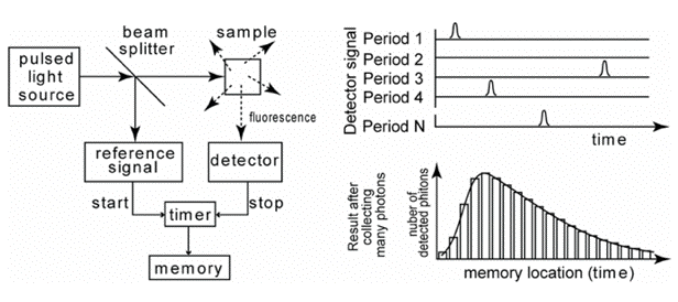
Figure 21. Schematics of time-correlated single photon counting. The arrival time of the first photon after an excitation pulse is measured and stored in memory. The histogram of many arrival times of photons represents the "fluorescence intensity versus time" curve.
The resulting signal is a convolution of the real decay over time (i.e., following the δ-pulse of excitation) of fluorescence intensity with the instrument response function (Figure 22).
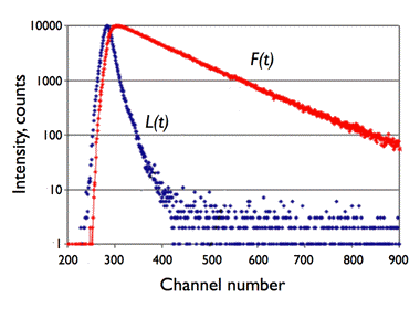
Figure 22. Illustration of the convolution principle. L(t) is the instrumental response function and F(t) is the experimental decay function. The channel number gives the time axis, as it corresponds to a certain time increment. F(t) is a convolution product of L(t) with the real decay function Fc(t):

Analysis of the measured fluorescence intensity curves and determination of fluorescence lifetimes are often performed by a nonlinear least-squares fitting method. Let us assume that a model function of a sum of two exponential terms adequately describes the course of fluorescence intensity with time. Such situation may occur, when the fluorophore exists in two distinct environments each characterised by its own fluorescence lifetime.

in which n=2, and
 1 and
1 and  1 are the amplitude and lifetime of component 1, and
  2 and
2 and  2 are the amplitude and lifetime of component 2. The result of the convolution of the model function with the instrument response function is fitted to the measured fluorescence intensity curves by optimising the parameters
  1,
1,  1 and
1 and  2,
2,  2.
2.
The resolution that can be achieved with TCSPC depends much on the light source and detector. Using mode-locked lasers in combination with microchannel-plate photomultipliers, instrument response function widths of thirty picoseconds are possible. This allows for the measurement of decay times in the range of ten to twenty picoseconds. Much cheaper diode lasers and light-emitting diodes (LEDs) give longer excitation pulses (width in the range 50-200 ps), but decay times of several hundred picoseconds can still be resolved.
In the phase-modulation method, the sample is excited by an intensity modulated light source, which can either be a xenon arc lamp, LED (see below) or a laser (pulsed or CW). The excitation is sinusoidal-modulated at angular frequency
 (rad/s). The fluorescence is delayed in phase and partially demodulated. The experimental quantities to be determined are the phase difference (
 ), and the modulation ratio (
 ), as shown in Figure 23.
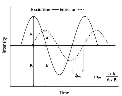
Figure 23. Determination of the phase difference () and modulation ratio (
) in the phase-modulation method.
For a single fluorescence lifetime, phase difference and modulation ratio are related to the lifetime (
 ) by:
) by:

For the precise determination of fluorescence lifetimes, the phase difference (
 ) and the modulation ratio (
 ) are measured as function of different frequencies
  . The curves can be analysed by the method of nonlinear least squares using theoretical expressions of the sine and cosine Fourier transforms of the δ-pulse response. The resolution of the phase-modulation method depends on the modulation frequency. Fluorescence lifetimes in the picosecond range can be measured using modulation frequencies between 2 and 10 GHz. For lifetimes in the 1-10 nanosecond range, modulation frequencies between 2 and 200 MHz are appropriate.
Luminescence From Semiconductor (Nano-)Crystals
Semiconductors: Until now we have treated light emission from aromatic molecules such as fluorescence and, in less detail, phosphorescence. A general term of light emission is luminescence, a term derived from the Latin "lumen", light, and introduced by the German scientist Eilhard Wiedemann in 1880 ("Lumineszenz"). Because luminescence from crystalline semiconductor materials has a completely different origin than that of fluorescence, it is worthwhile to pay attention to it, as we are surrounded nowadays by many applications of them.
To understand how semiconductors work we must have background knowledge in solid-state physics. That is beyond the scope of this module, and we prefer to give a qualitative picture of the physics behind semiconductors. A semiconductor is a material that has an electrical conductivity between that of a conductor and an insulator, that is, generally in the range 103 Siemens/cm (conducting) to 10-8 S/cm (non-conducting). Devices made from semiconductor materials are used in modern electronics, including computers, telephones, LCD displays, etc. Semiconductors have also found applications in opto-electronics and photophysics. Below we will briefly describe the working principles of quantum dots, light emitting diodes (LEDs), diode lasers and solar cells.
There is another motivation to know more about semiconductors, especially solar cells. The working principle of solar cells shows a remarkable analogy with that of the photosynthetic apparatus. Plants use radiation in the wavelength range of 400-700 nm to reduce CO2 to glucose, with the concomitant oxidation of water to O2. The radiation energy is in the range of the band gap of many semiconductor materials (Table 3).
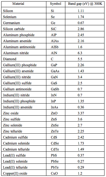
Table 3. Some semiconductor materials and their band gaps.
[adapted from Wikipedia: Band Gap]
This photosystem consists of protein complexes, which combine light harvesting proteins and reaction centers. The light harvesting complex having bound a large number of chlorophylls and carotenoids, absorbs solar energy and rapidly transfers this energy to the reaction center, which is a special pair of two chlorophyll molecules. Efficient light harvesting requires that energy must be transferred via weak (Förster-type) and strong (exciton-type) coupling mechanisms. This is analogous to the creation of electrons, holes and excitons in semiconductor materials after illumination, which are transported efficiently in the crystal lattice to a p-n junction (see below). The function of a p-n junction may be compared to that of the reaction center of the photosystem, since charge carriers are separated in both systems. Negative charge carriers are electrons in both systems. Positive carriers are holes in semiconductors, and protons in reaction centres. Both photosystems and solar cells must operate reversibly. They share, therefore, the same process of recombination of charge carriers.
Impregnating impurities into their crystal lattice may easily modify the conductivity of semiconductors. The process of the controlled adding of impurities to a semiconductor is known as 'doping'. The amount of impurity, or dopant, added to a pure semiconductor varies its level of conductivity, and also its band gap. By incorporating impurity atoms into the crystal lattice of pure semiconductors, the electrical conductivity may be varied not only by the number of impurity atoms but also, by the type of impurity atom.
In general, dopants that produce the desired controlled changes are classified as either electron acceptors or donors. A donor atom donates weakly bound valence electrons to the material creating excess negative charge carriers. These weakly bound electrons can move in the crystal lattice relatively freely, and can facilitate conduction in the presence of an electric field. Conversely, an activated acceptor produces an electron hole (usually referred to simply as a hole), which carries a positive charge. The holes do not actually move, but a neighboring electron can move to fill the hole, leaving a hole at the place that the electron occupied previously. In this way, holes can also move freely in the crystal lattice. Both conduction-band electrons and valence-band holes contribute to electrical conductivity. Semiconductors doped with donor impurities are called n-type (n meaning negative), while those doped with acceptor impurities are known as p-type (p meaning positive).
Quantum mechanical theory predicts that electrons in semiconductors can have energies only within certain bands corresponding to electrons tightly bound to the atomic nuclei of the material, and the free electron energy, which is the energy required for an electron to escape entirely from the material. Each energy band corresponds to a large number of discrete quantum states of the electrons. Most of the states with low energy (closer to the nucleus) are filled with electrons, up to a particular band, which is called the valence band, and which is also filled with electrons. Semiconductors and insulators are distinguished from metals because the valence band in the semiconductor materials is nearly filled under usual operating conditions, thus causing more electrons to be available in the conduction band, which is the band immediately above the valence band (and empty at absolute zero temperature, 0 K). The ease with which electrons in a semiconductor can be excited from the valence band to the conduction band depends on the band gap between the bands, and it is the size of this energy band gap that serves as an arbitrary dividing line (roughly 4 eV) between semiconductors and insulators (Figure 24).

Figure 24. Energy bands of electrons in a metal, semiconductor and insulator. The Fermi level refers to the energy of the highest occupied quantum state in a system of fermions at absolute zero temperature. A fermion is any particle that has an odd half-integer (like 1/2, 3/2, and so forth) spin. [From Wikipedia: Electronic Band Structiure]
p-n Junctions: A p-n junction is a junction formed by joining p-type and n-type semiconductors together in very close contact (Figure 25). The term junction refers to the boundary interface where the two regions of the semiconductor meet. Although they can be constructed of two separate pieces, p-n junctions are more often created in a single crystal of semiconductor by growing a layer of crystal doped with one type of dopant on top of a layer of crystal doped with another type of dopant.


Figure 25. p-n Junctions in silicon in an open circuit (top), forward-bias (bottom, left), and reverse-bias circuits (bottom, right). [From Wikipedia: p-n Junction]
The p-n junction possesses some interesting properties, which have useful applications in modern electronics. A p-doped semiconductor is relatively conductive. The same is true of an n-doped semiconductor, but the junction between them is a non-conductor. This non-conducting layer, called the depletion (or space charge) region, arises because the electrical charge carriers in doped n-type and p-type semiconductors (electrons and holes, respectively) attract and eliminate each other in a process called recombination. Transport of charge carriers can occur in two ways. One mode of transport is by 'drift', which is caused by an electrostatic field across the device. The other mode of transport is by diffusion of carriers from zones of high carrier concentration to zones of low carrier concentration. Drift and diffusion have opposite directions. Figure 26 gives a schematic picture of a p-n junction. P-n junctions are essentially electronic diodes and are elementary building blocks of almost all opto-electronic devices such as LEDs, diode lasers, solar cells, etc.
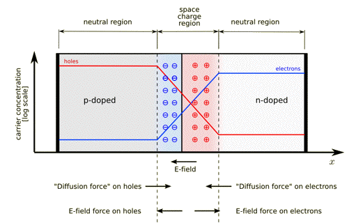
Figure 26. A p-n junction in thermal equilibrium with zero bias voltage applied. Blue and red lines indicate the concentration of electrons and holes, respectively. Gray and white regions have neutral charges. The light red zone is positively charged (holes). The light blue zone is negatively charged (electrons). The direction of the electric field is shown on the bottom. Also shown are the electrostatic force on electrons and holes (drift), and the direction in which the diffusion tends to move electrons and holes. [From Wikipedia: p-n Junction]
Luminescence of Semiconductors: By the absorption of a photon, an electron can be promoted from the valence band into the conduction band. Electrons excited to the conduction band also leave behind electron holes in the valence band.
Luminescence can originate from direct light absorption, since recombination of the excited electron with the hole in the valence band is accompanied by light emission. Luminescence can also be created by excitons. An exciton is an electron-hole pair, bound by Coulomb forces, with the electron in the conduction band, and the hole in the valence band. Since an exciton is a bound state of an electron and a hole, the overall charge for this quasi-particle is zero. Hence it carries no electric current. The whole exciton can move through the molecular crystal, and impurities (so-called carrier traps) are sometimes added to stabilize the exciton at one position. With this additional kinetic energy the excitonic energy may lie above the band-gap. This extra energy can be released by radiation. This light emission in semiconductors is taking place at lower temperature, when the Boltzmann factor (κBT) is less than the exciton binding energy.
In Figure 27, we have redrawn the quantum-mechanical band scheme to understand the luminescence of semiconductors.
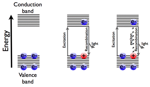
Figure 27. Band scheme of semiconductors, and the two ways of light emission.
Quantum Dots: Nanometer-sized crystals of certain semiconductors, such as cadmium selenide (CdSe), have interesting luminescent properties. After photon absorption, the wavelength of luminescence depends on the nature of the semiconductor material, and on the size of the crystal. The light emission is due to a phenomenon known as quantum confinement. Therefore these nanocrystals are called 'quantum dots'. In quantum dots, electrons, holes and excitons are confined in all three spatial dimensions. The smaller the quantum dot is, the shorter is the emission wavelength. The color of luminescence of CdSe quantum dots varies from violet to red, when the size increases from 2 nm to 7 nm. The emission color of quantum dots can be tuned from the visible throughout the infrared by the careful choice of materials and sizes (Figure 28). The quantum yield of luminescence can be increased by coating the quantum dot with a layer of zinc sulfide (ZnS), which has a much larger band gap (see Table 3), and finally with a polymer. This protective layer will reduce non-radiative decay processes responsible for the low quantum yield.
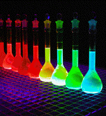
Figure 28. Luminescence of various quantum dots illuminated with UV light.
Over the past decade, quantum dots have been used in the confocal fluorescence microscopy of cells, thereby replacing organic fluorescent dyes. The improved photo-stability of quantum dots allows acquisition of many consecutive two-dimensional confocal images that can be reconstructed into a high-resolution three-dimensional confocal image. Another application taking advantage of their photostability is the tracking of certain biological molecules attached to quantum dots ("biosensors") in living cells and animals (mice) over extended periods of time (even months). First attempts have been made to use quantum dots for tumor targeting. One of the remaining issues with quantum dot probes is their in vivo toxicity, as they have to be excited with UV light. Quantum dots with a stable polymer coating seem to be essentially nontoxic.
Light Emitting Diode (LED): An LED consists of a chip of semiconducting material doped with impurities to create a p-n junction. When the p-n junction is forward biased (switched on) (Figure 25), current flows easily from the p-side (anode) to the n-side (cathode), but not in the reverse direction. Charge carriers - electrons and holes - flow into the junction from electrodes with different voltages. When an electron meets a hole, it falls into a lower energy level, and releases energy in the form of a photon (Figure 29). This effect is called electroluminescence and the color of the light is determined by the band gap energy of the materials forming the p-n junction. An LED is usually small in area (less than 1 mm2), and integrated optical components are used to shape its radiation pattern and assist in reflection to improve the output (Figure 29).
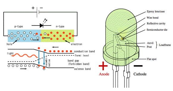
Figure 29.Working principle (left), and schematics of an LED (right). [From Wikipedia: LED]
LEDs present many advantages over other light sources, including lower energy consumption, longer lifetime, smaller size, faster switching and greater reliability. LED development began with infrared and red devices made with gallium arsenide (see Table 3). Advances in material science have made possible the production of LEDs having band gaps with energies corresponding to near-infrared, visible or ultraviolet light. LEDs made from silicon or germanium are not effective, since electrons and holes recombine by a non-radiative transition, producing no light emission.
Diode Laser: Like many other semiconductor devices, a diode laser is formed by doping a very thin layer on the surface of a crystalline wafer. The crystal is doped to produce an n-type region and a p-type region, one above the other, resulting in a p-n junction. Charge injection distinguishes diode lasers from all other, optically pumped lasers. Therefore diode lasers are called "injection lasers". The initial mode of action is not different from that of an LED. Electron-hole recombination below a laser threshold may result in spontaneous emission, as in an LED. Spontaneous emission is necessary to initiate laser oscillation. In the absence of stimulated emission, electrons and holes may coexist in proximity to one another for a certain time before they recombine. This characteristic time is termed the "recombination time" (about a nanosecond for typical diode laser materials). Then a nearby photon with energy equal to the recombination energy can cause recombination by stimulated emission. This generates another photon of the same frequency, traveling in the same direction, with the same polarization and phase as the first photon. This means that stimulated emission causes gain in an optical wave in the injection region. The gain increases as the number of electrons and holes injected across the junction increases.
As in other lasers, the gain region is surrounded with an optical cavity to form a laser. In the simplest form of a diode laser, an optical waveguide is made on the crystalline wafer, such that the light is confined to a relatively narrow line. The two ends of the crystal are cleaved to form perfectly smooth, parallel edges, forming an optical resonator. Photons emitted into a mode of the waveguide will travel along the waveguide, and be reflected several times from each end face (mirror) before they are emitted. As a light wave passes through the cavity, it is amplified by stimulated emission, but light is also lost due to absorption, and by incomplete reflection from the end mirrors. Finally, if there is more amplification than loss, the diode begins to perform laser action. Due to diffraction, the beam diverges rapidly in vertical and lateral directions after leaving the chip. A lens must be used in order to form a collimated beam like that produced by a laser pointer.
In Figure 30, a diagram of a double hetero-structure diode laser is shown. In this device, a layer of low band-gap material is sandwiched between two high band-gap layers. One commonly used pair of materials is gallium arsenide (GaAs) with aluminum-doped gallium arsenide (AlGaAs). Each of the junctions between different band gap materials is called a hetero-structure, hence the name "double hetero-structure" laser or DH laser. The advantage of a DH laser is that the active region where free electrons and holes exist simultaneously, is confined to the thin middle layer with lower band gap energy. This means that many more of the electron-hole pairs can contribute to amplification. In addition, light is reflected from the hetero-junction; hence, the light is confined to the region where the amplification takes place.
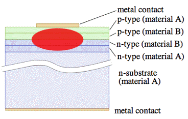
Figure 30. Diagram of front view of a double heterostructure laser diode (not to scale). Material A is, for instance, AlGaAs (band gap ~2.8 eV). Material B is, for instance, GaAs (band gap 1.43 eV). [From Wikipedia: Diode Laser]
The relatively low cost of mass-produced diode lasers makes them attractive for a wide range of applications in diverse areas. The small size of diode lasers is also advantageous. Diode lasers are used in fiber optics communication, optical data recording and barcode readers. Red and green lasers are common as laser pointers. Both low and high-power diode lasers are used extensively in the printing industry, both for scanning of images and for very high-resolution printing plate manufacturing. Infrared and red diode lasers are common in CD and DVD players. Diode lasers are also indispensable light sources in confocal fluorescence microscopy and time-resolved fluorescence spectroscopy. High-power diode lasers are used for pumping other, solid-state lasers like Ti-Sapphire. Medical applications include, among others, photodynamic therapy to photo-activate porphyrin derivatives as anti-cancer agents.
Solar Cells: A solar cell is a device that converts the energy of sunlight directly into electricity by the photovoltaic effect. In contrast to LEDs and diode lasers that produce light, solar cells use light to produce electricity. An assembly of solar cells makes a solar panel. Construction of solar cells has a long history, starting in the 1880s, and resulting in semiconductor (silicon) devices with a sunlight energy conversion efficiency of around 6% in the 1950s. Highly effective hetero-structure solar cells were created from 1970 on, until conversion efficiencies have been reached close to 40%. A current challenge to bring down the cost of solar energy is to increase the photovoltaic efficiency.
Solar cells are essentially p-n junctions under illumination. Light generates electrons and holes on both sides of the junction, in the n-type emitter and in the p-type base. Charges build up on either side of the junction and create an electric field. The generated electrons (from the base) and holes (from the emitter) then diffuse to the junction and are swept away by the electric field, thus producing electric current across the device. The electric currents of the electrons and holes reinforce each other, since these particles carry opposite charges. The p-n junction, therefore, separates the carriers with opposite charge, and transforms the generation current between the bands into an electric current across the p-n junction. (Figure 31).
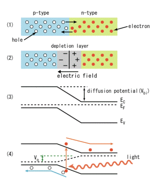
Figure 31. Photovoltaic effect on p-n junctions. Panels 1 and 2 are explained in Figure 26. In panel 3 the electric fields are plotted. EF is the Fermi level. In panel 4 the actual current is generated by light. Note that electrons and holes move in opposite directions. [From Wikipedia: Solar Cells]
Ohmic-metal semiconductor contacts are made to both n-type and p-type sides of the solar cell (Figure 32).
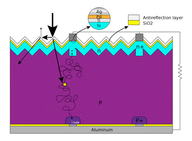
Figure 32. Basic structure of a silicon based solar cell, and its working mechanism. The electrodes are connected to an external resistance load. [From Wikipedia: Solar Cells]
Electrons that are created on the n-type side of the junction may travel through the wire, power the load, and continue through the wire until they reach the p-type semiconductor-metal contact (aluminum). Here they recombine with a hole. The hole was either created as an electron-hole pair on the p-type side of the solar cell or swept across the junction after being created at the n-side. The voltage measured is equal to the difference in energy levels of the minority carriers, i.e., electrons in the n-type portion and holes in the p-type portion (V0 in panel 4 of Figure 31).
Suggested Reading
Birks, J.B., Photophysics of Aromatic Molecules, Wiley-Interscience, London, 1970.
Cantor, C.R. and Schimmel, P.R., Biophysical Chemistry, Part II: Techniques for the Study of Biological Structure and Function, W.H. Freeman, San Francisco, 1980.
Engelborghs, Y. and Visser, A.J.W.G. Visser (eds.), Fluorescence Spectroscopy and Microscopy: Methods and Protocols, Methods in Molecular Biology, vol. 1076, Springer Science + Business Media, LLC, 2014.
Jameson, D.M., Introduction to Fluorescence, CRC Press, 2014.
Lakowicz, J.R., Principles of Fluorescence Spectroscopy, 3rd ed., Springer, New York, 2006.
Saleh, B.E.A. and Teich, M.C., Fundamentals of Photonics, 2nd ed., John Wiley & Sons, Hoboken, New Jersey, 2007.
Steinfeld, J.I., Molecules and Radiation. An Introduction to Modern Molecular Spectroscopy, Harper & Row Publishers, New York, 1974.
Valeur, B. and Berberan-Santos, M.N., Molecular Fluorescence, 2nd ed., Wiley-VCH, Weinheim, 2012.
Many topics treated in this module can be found in: Wikipedia.
A very useful review on cellular applications of quantum dots can be found in: Michalet, X., Pinaud, F.F., Bentolila, L.A., Tsay, J.M., Doose, S., Li, J.J., Sundaresan, G., Wu, A.M., Gambhir, S.S. and Weiss, S., Quantum Dots for Live Cells, in Vivo Imaging, and Diagnostics, Science 307, 538-544, 2005.
Fluorescence microscopy, and history can be found in: Microscopy.
A wide selection of fluorescent probes can be found in: Molecular Probes.
03/15/10
12/03/10
03/24/14